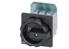

Today we're working with a classic but often overlooked component: the EDAC 626 series right-angle D-sub connector, specifically the 25-position model (626-025-662-543). This isn't just a simple connector; it's a robust, solder-cup, right-angle PCB mount receptacle. We'll design a practical interface board that conditions digital signals from an industrial sensor cluster, routing them through this D-sub for connection to a main control unit. This component is perfect for our tutorial because it forces us to consider mechanical footprint, hand-soldering techniques for a multi-pin connector, and the signal integrity implications of routing multiple traces to a dense, legacy connector format. Its right-angle nature saves panel space, a common real-world constraint.
Our design requirements are to create a PCB that accepts 12 digital input channels (24V nominal, compliant with IEC 61131-2 Type 1/3 standards) via screw terminals, conditions them to 3.3V CMOS logic levels, and outputs them through the 25-pin D-sub to a data logger. Key specifications include: input protection against ±30V transients, optical isolation for noise immunity, and a maximum data rate of 1 Mbps per channel. The EDAC connector will carry the 12 data lines, a common ground, a +5V output to power external line drivers, and several spare pins for future use. We must adhere to the connector's datasheet dimensions for the PCB cutout and pad pattern, ensuring a secure mechanical fit.
The step-by-step design process begins with the mechanical layout. We obtain the connector's datasheet and import its recommended PCB footprint, paying close attention to the non-plated mounting hole locations and the board edge cutout for the connector shell. We place this first. Next, we design the input stage. Each channel requires a current-limiting resistor, a clamping TVS diode for the ±30V protection, and a reverse-polarity protection diode. Calculation for the input resistor (R_in) is based on the worst-case input voltage and the optocoupler LED current. If our optocoupler (e.g., SFH618A) has a typical forward voltage (V_f) of 1.2V at 5mA, and our maximum input is 30V: R_in = (30V - 1.2V) / 0.005A = 5760Ω. We select a standard 5.6kΩ, 1W resistor for margin. The output side of the optocoupler uses a pull-up resistor to 3.3V; a 4.7kΩ resistor provides a good balance of speed and power consumption.
Our component selection rationale for the BOM balances cost, availability, and robustness. The EDAC 626-025-662-543 connector is chosen for its proven reliability in industrial environments and its solder-cup terminals, which are more forgiving for hand prototyping than surface-mount versions. For isolation, we select the SFH618A optocoupler for its 5kVrms isolation rating and manageable speed. The TVS diodes are SMAJ series unidirectional 33V types, providing robust clamping. The voltage regulator is a classic LM7805 to supply the optocoupler input side and the +5V output pin on the D-sub, fed from an external 24V supply. All passive components are through-hole for ease of manual assembly, with 1206-size resistors and capacitors used where possible for their ease of handling.
For simulation tips, focus on two key areas: the transient protection network and the optocoupler's dynamic response. Use SPICE to simulate a voltage spike on an input channel. Inject a 30V, 1ms pulse through the 5.6kΩ resistor and monitor the voltage at the TVS diode/optocoupler node; verify it clamps safely below the diode's breakdown. For timing, model the optocoupler as a simple RC network (a 100kΩ resistor and a 4pF capacitor can approximate the SFH618A's slow switching). This will show the rise/fall times and potential for pulse widening at your 1Mbps target. Pay particular attention to the ground bounce and crosstalk that could be introduced by the dense pinout of the D-sub connector in your layout; while hard to simulate perfectly, ensure your PCB design has a solid ground plane and routes sensitive signals away from high-current paths.
The prototype build starts with a carefully inspected PCB, verifying the mechanical cutout matches the physical connector. Always solder the right-angle D-sub connector first. Use a vise to hold the board vertically, apply flux to the solder cups, and carefully feed solder from a fine gauge roll, ensuring it wicks into the cup and forms a solid fillet on the PCB pad. This requires a temperature-controlled iron set to about 700°F (370°C). After the connector is secured, populate the remaining components. For testing, use a variable power supply and a function generator. Gradually increase input voltage on each channel from 0V to 24V while monitoring the 3.3V output with an oscilloscope. Verify the threshold logic levels and then inject short-duration overvoltage pulses to confirm protection circuitry activation.
Performance verification involves quantifying channel-to-channel skew, maximum data rate, and isolation breakdown. Use a multi-channel pattern generator to send identical 500kHz square waves to all 12 inputs and measure the time difference between output edges on the scope. This skew, often introduced by slight variations in optocoupler response, should be less than 100ns for our application. To test the isolation, perform a hipot test at 1500V AC between the input common and the output ground, ensuring no breakdown occurs. Optimization may involve swapping pull-up resistor values to sharpen rise times if the data rate is marginal, or adding small (10-100pF) capacitors across the optocoupler outputs to filter high-frequency noise picked up in the cable connected to the D-sub, a common issue in electrically noisy environments.