Interpreting the datasheet for the SiTime SIT9365AC-1E1-25E168.040678, a MEMS-based 168.040678 MHz LVPECL oscillator, requires a detailed understanding of its specifications to ensure optimal performance in high-frequency, low-jitter applications such as high-speed serial links, networking equipment, and advanced test instrumentation. This guide will walk through the critical sections of the component's documentation, translating technical parameters into practical design considerations.
Beginning with the key electrical specifications, the core parameter is the output frequency of 168.040678 MHz, which is derived from SiTime's programmable MEMS resonator platform, offering exceptional frequency stability of ±25 ppm. This stability encompasses all deviations over temperature, supply voltage variation, and aging over the component's lifetime, a significant advantage over traditional quartz crystals. The output logic is LVPECL (Low-Voltage Positive Emitter-Coupled Logic), which mandates careful attention to termination. The datasheet will specify output voltage levels (VOH and VOL) and differential swing (typically around 800mV). In practice, this means the designer must implement a 50-ohm transmission line environment with a Thevenin termination (e.g., 130Ω to VCC-2V and 82Ω to ground) at the receiver to prevent signal reflections and ensure clean edge rates. Another paramount specification is phase jitter, typically given in femtoseconds or picoseconds RMS over specific integration bands (e.g., 12 kHz to 20 MHz). For a 168 MHz clock driving a SerDes PHY, low phase jitter is non-negotiable to maintain low bit-error rates. The supply voltage (VDD) and current consumption (ICC) define the power envelope; this oscillator typically operates from a 3.3V rail, and its low power consumption is a direct benefit of the MEMS architecture.
The absolute maximum ratings table defines the stress limits beyond which permanent damage may occur. For this component, these include the maximum supply voltage, storage temperature range, and the allowable voltage on any pin relative to ground. It is crucial to note that these are not operating conditions. A critical derating consideration involves the operating temperature range, specified as -40°C to +85°C for the industrial-grade part. While the oscillator will function within this range, key parameters like frequency stability and supply current will vary. The ±25 ppm stability is guaranteed across this entire temperature span. Designers must also consider voltage derating; while the absolute maximum VDD might be 4.0V, the recommended operating condition is 3.3V ±5% or ±10%. Consistently operating near the absolute maximum voltage will accelerate aging and potentially degrade reliability.
Analyzing the typical application circuit provided in the datasheet is essential for successful implementation. The circuit will show the mandatory decoupling capacitors on the VDD pin, usually a combination of a bulk capacitor (e.g., 10µF) and a low-inductance ceramic capacitor (e.g., 0.1µF) placed extremely close to the device to filter noise. For the LVPECL outputs, the diagram will illustrate the proper differential termination network located as close as possible to the receiver's input pins. It will also show the connection for the OE (Output Enable) pin, if present, which allows for clock gating. A common oversight is leaving unused outputs improperly terminated; for a differential output, if only one side is used, the complementary output must still be terminated properly to maintain signal integrity.
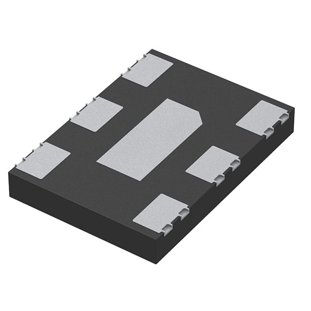
The pin configuration and package considerations for this 5-pin ceramic or metal surface-mount package (typically 5.0x3.2mm) demand careful PCB layout. Pin 1 is usually denoted by a dot or bevel and is often the VDD pin. The two differential output pins (OUT and OUT#) must be routed as a tightly coupled differential pair with controlled impedance (50Ω single-ended, 100Ω differential) and equal length to minimize skew. The GND pin requires a low-impedance connection to the board's ground plane via multiple vias directly at the pad. The small package size underscores the importance of thermal expansion coefficient matching between the component, solder, and PCB to mitigate mechanical stress, which the MEMS design is inherently more resistant to than quartz.
While MEMS oscillators are highly resilient, thermal management guidelines remain relevant. The datasheet will specify a junction-to-ambient thermal resistance (θJA). Although power dissipation is low, calculating the junction temperature rise (Tj = Ta + (PD * θJA)) is necessary in high-ambient-temperature environments. Ensuring adequate ground plane connection under the package acts as a heat spreader. Avoid placing high-heat-generating components adjacent to the oscillator, as localized board heating can indirectly affect performance despite the component's excellent temperature stability.
Finally, understanding how to read the timing diagrams and characteristic curves is vital for system timing analysis. The timing diagram will detail the output enable/disable times (tEN, tDIS), which define the latency from the OE pin toggle to a valid clock output. For LVPECL, the rise and fall times (tr, tf) are extremely fast, often in the sub-nanosecond range, as shown on the diagrams; these fast edges necessitate the previously emphasized proper termination. Characteristic curves graphically show the behavior of parameters like frequency stability over temperature, supply current vs. voltage, or phase jitter vs. supply noise. These curves provide insight beyond the typical/max/min table values, allowing designers to visualize performance trends and margins across the entire operating window, ensuring robustness in their specific application environment.